
This document introduces the IDT71V3556/58 device's product characteristics, including device type, working voltage, storage capacity, storage speed, interface type, etc.
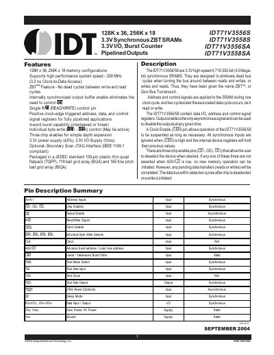
The IDT71V3556/58 family provides 3.3 V high‑speed synchronous SRAMs with Zero Bus Turnaround (ZBT) to eliminate dead cycles between write and read operations. Available in 128 K×36 and 256 K×18 memory configurations, the devices support up to 200 MHz system speed and feature a single read/write control pin, 4‑word burst capability, and individual byte‑write control.
The parts are offered in JEDEC‑standard 100‑pin TQFP, 119‑ball BGA and 165‑ball fine‑pitch BGA packages. They include three chip‑enable pins, a clock‑enable pin, and an optional JTAG boundary‑scan interface. Recommended operating temperatures range from 0 °C to +70 °C (commercial) or –40 °C to +85 °C (industrial), with a 3.3 V core and I/O supply.
| Memory configurations | 128 K×36 or 256 K×18 |
|---|---|
| Maximum operating frequency | 200 MHz (3.2 ns clock‑to‑data) |
| Supply voltage (core) | 3.3 V (typical) |
| Supply voltage (I/O) | 3.3 V (typical) |
| Operating temperature (commercial) | 0 °C to +70 °C |
| Operating temperature (industrial) | -40 °C to +85 °C |
| Package types | 100‑pin TQFP, 119‑ball BGA, 165‑ball fBGA |
| Chip‑enable pins | Three (CE1, CE2, CE2) |
ZBT (Zero Bus Turnaround) eliminates dead cycles between write and read operations, allowing continuous data flow.
The SRAM has three chip‑enable pins: CE1, CE2, and a second CE2 pin.
The device supports up to 200 MHz operation (3.2 ns clock‑to‑data access).