
The IDT2308A is a high-speed phase-lock loop (PLL) clock multiplier designed for high-speed clock distribution and multiplication applications. It has two banks of four outputs each that are controlled via two select addresses. By proper selection of input addresses, both banks can be put in tri-state mode. In test mode, the PLL is turned off, and the input clock directly drives the outputs for system testing.
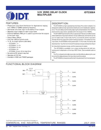
The IDT2308A is a high‑speed phase‑lock loop (PLL) clock multiplier that distributes one input clock to two banks of four outputs. It provides selectable 1×, 2× or 4× multiplication, separate enable for each bank, and optional high‑drive versions. The device operates from a 3.3 V supply and is available in SOIC and TSSOP packages.
The datasheet details pin configurations, absolute maximum ratings, electrical characteristics, switching performance, and recommended test circuits. It also lists commercial (0 °C to +70 °C) and industrial (‑40 °C to +85 °C) operating temperature ranges, and ordering information for the various part numbers.
| Supply Voltage Range | -0.5 V to +4.6 V |
|---|---|
| Input Voltage Range (REF) | 0.5 V to 4.55 V |
| Continuous Output Current | +50 mA |
| Cycle‑to‑Cycle Jitter | <200 ps |
| Industrial Operating Temperature | -40 °C to +85 °C |
The device can be powered with a supply voltage from –0.5 V up to +4.6 V.