
The document describes a N-Channel Enhancement Mode HiPerFETTM MOSFET product from IXYS. This product belongs to the HDMOSTM family and features high dv/dt, low trr. It uses a silicon chip on a Direct-Copper-Bond substrate, which allows for high power dissipation, isolated mounting surface, and 2500V electrical isolation. Additionally, the product has low drain to tab capacitance (<35pF), low RDS (on), and a rugged polysilicon gate cell structure.
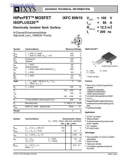
This document provides technical specifications for the IXYS IXFC 80N10 HiPerFETTM MOSFET. The device is an electrically isolated back surface component designed for high power dissipation with a silicon chip on a Direct-Copper-Bond substrate.
Key features include low drain to tab capacitance, rugged polysilicon gate cell structure, and Unclamped Inductive Switching (UIS) rating. It is intended for applications such as DC-DC converters, battery chargers, switched-mode power supplies, and AC motor control.
| Max Drain-Source Voltage (VDS) | 100 V |
|---|---|
| Max Continuous Drain Current (ID) | 80 A |
| Max Pulse Current (IDM) | 320 A |
| Typical On-Resistance (RDS(on)) | 12.5 mΩ |
| Max Power Dissipation (PD) | 230 W |
| Operating Junction Temperature Range | -55 ... +150 °C |
| Electrical Isolation Voltage | 2500 V~ |
The device is suitable for DC-DC converters, battery chargers, switched-mode and resonant-mode power supplies, DC choppers, and AC motor control.
No, it features easy assembly with no screws or isolation foils required.
The junction temperature range extends from -55°C to +150°C.