
This document describes the features and characteristics of the ASI AVD0.5P NPN Silicon RF Power Transistor, including minimum current gain, maximum voltage, and power.
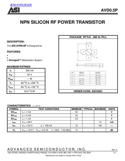
The ASI AVD0.5P is an NPN silicon RF power transistor designed with the Omnigold™ Metalization System. It is packaged in a .280 4L Pill style.
Key electrical characteristics include a maximum collector current of 300 mA and a typical gain (hfe) ranging from 10 to 15 at Vce = 5.0 V and Ic = 100 mA.
| Collector Current (Ic) | 300 mA |
|---|---|
| Collector-Emitter Voltage (Vee) | 20 V |
| Power Dissipation (Poiss) | ~5 W |
| Operating Temperature Range | -65 °C to +200 °C |
| Storage Temperature (Tste) | -65 °C to +150 °C |
| Thermal Resistance (uc) | 35.0 °C/W |
| Collector-Base Breakdown Voltage (BVcpo) | 50 V |
| Collector-Emitter Breakdown Voltage (BV ceo) | 20 V |
| Emitter-Base Breakdown Voltage (BVeso) | 3.5 V |
| Collector Cutoff Current (Ices) | 1.0 mA |
| Gain (hfe) Typical | 15 |
| Frequency Range | 1025 - 1150 MHz |
The ASI AVD0.5P is designed for use as an NPN silicon RF power transistor.
The device can operate from -65 °C to +200 °C.