
The document describes the features and characteristics of the ASI 1020 NPN Silicon RF Power Transistor. The transistor is designed for general purpose Class C power amplifier applications up to 1500 MHz.
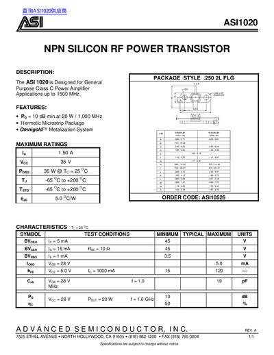
The document is a single-page datasheet for the ASI1020, an NPN silicon RF power transistor. It specifies that the device is designed for general-purpose Class C power amplifier applications operating up to 1500 MHz.
Key features include a hermetic microstrip package and an Omnigold™ metalization system. The datasheet provides electrical characteristics such as breakdown voltages (BVCBO, BVCER), current gain (hFE), and output power gain (PG) at specific test conditions.
| Frequency Range | up to 1500 MHz |
|---|---|
| Collector-Base Breakdown Voltage (BVCBO) | 45 V minimum |
| Collector-Emitter Breakdown Voltage (BVCER) | 45 V minimum |
| Emitter-Base Breakdown Voltage (BVEBO) | 3.5 V minimum |
| Collector Cutoff Current (ICBO) | 5.0 mA maximum |
| DC Current Gain (hFE) | 15 to 120 typical |
| Output Power Gain (PG) | 10 dB minimum at 20 W / 1,000 MHz |
| Maximum Collector Current (IC) | 1.50 A |
| Maximum Supply Voltage (VCC) | 35 V |
| Maximum Power Dissipation (PDISS) | 35 W @ TC = 25 OC |
| Operating Junction Temperature Range (TJ) | -65 OC to +200 OC |
The ASI1020 is designed for general purpose Class C power amplifier applications up to 1500 MHz.
The minimum gain is 10 dB when operating at 20 W output power and 1,000 MHz frequency.
The maximum junction temperature (TJ) ranges from -65 OC to +200 OC.