
The HD74ALVCH16831 is a 1-to-4 address register/driver designed for operation with a VCC range of 2.3V to 3.6V. It is suitable for applications where a single address bus drives four separate memory locations. The HD74ALVCH16831 can function as either a buffer or a register, depending on the logic level of the select (SEL) input. In buffer mode (SEL logic high), the outputs mirror the inputs and are controlled by two output enable (OE) controls. Each OE control operates two groups of nine outputs. In register mode (SEL logic low), the device operates as an edge-triggered D-type flip flop. On the positive transition of the clock (CLK) input, data set up at the A inputs is stored in internal registers. The OE controls function the same way as in buffer mode. When OE is logic low, the outputs are in a normal logic state (either high or low logic level). When OE is logic high, the outputs enter a high impedance state. To ensure the high impedance state during power up or power down, OE should be pulled up to VCC using a pullup resistor, with the minimum value determined by the driver's current sinking capability. SEL and OE do not affect the internal operation of the flip flops, allowing for retention of old data or entry of new data while the outputs are in the high impedance state.
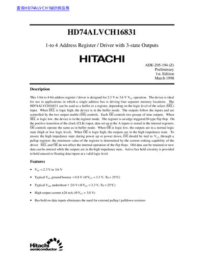
The HD74ALVCH16831 is a 1-bit to 4-bit address register/driver designed for 2.3V to 3.6V operation. It functions as a buffer or register based on the SEL input level. In buffer mode, outputs follow inputs and are controlled by OE. In register mode, it acts as an edge-triggered D-type flip-flop. The device includes bus hold circuitry to eliminate need for external pull-up/pull-down resistors.
Key features include high output current (+24mA at 3.0V), low power dissipation, and compatibility with TTL/CMOS logic. It is suitable for applications where a single address bus drives multiple memory locations. The datasheet includes pin configuration, electrical characteristics, switching performance, and package dimensions.
| Supply Voltage | 2.3 V to 3.6 V |
|---|---|
| Output Current | +24 mA (@Vcc = 3.0 V) |
| Operating Temperature | -40°C to 85°C |
| Maximum Clock Frequency | 150 MHz |
| Output Enable Time | 1.1 ns to 5.5 ns |
| Package Type | TVSOP |
The device operates from 2.3 V to 3.6 V.
The maximum clock frequency is 150 MHz.
The device can deliver up to +24 mA at 3.0 V.
The device operates from -40°C to 85°C.