
The AO4408 is a N-channel enhancement mode field effect transistor with a maximum drain-source voltage of 30V and a maximum drain current of 12A. Typical on-resistance is 13mΩ (VGS = 10V) and typical on-resistance is 16mΩ (VGS = 4.5V). The AO4408 uses advanced trench technology to provide excellent RDS(ON), low gate charge and fast switching. This device makes an excellent high side switch for notebook CPU core DC-DC conversion. AO4408L(Green Product) is offered in a lead-free package.
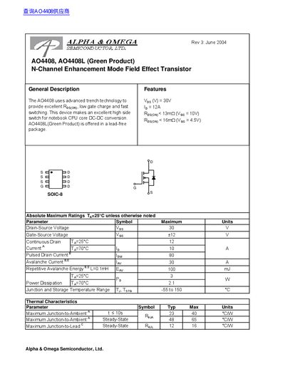
This handbook describes the AO4408L N‑Channel Enhancement Mode Field Effect Transistor, highlighting its trench technology, low gate charge, and fast switching suitable for high‑side switching applications. The document lists key features such as a 30 V drain‑source voltage, 12 A continuous drain current, and lead‑free packaging.
Detailed electrical and thermal characteristics are presented, including absolute maximum ratings, static and dynamic parameters, and switching performance. Typical curves illustrate on‑resistance versus drain current, gate‑charge behavior, and avalanche capability, helping designers evaluate the device for their circuits.
| Drain-Source Voltage (VDS) | 30 V |
|---|---|
| Gate-Source Voltage (VGS) | +12 V |
| Continuous Drain Current (ID) @ 25°C | 12 A |
| Pulsed Drain Current | 80 A |
| Avalanche Current | 30 A |
| Power Dissipation (PD) @ 25°C | 2.1 W |
| Junction Temperature Range | -55 °C to 150 °C |
| Input Capacitance (Ciss) | 1020 pF |
| Output Capacitance (Coss) | 320 pF |
| Total Gate Charge (Qg) | 10.3 nC (typ) |
The AO4408L is rated for a maximum drain‑source voltage of 30 V.
It can continuously conduct up to 12 A at an ambient temperature of 25 °C.
The typical on‑resistance is about 13 mΩ under those conditions.
The input capacitance (Ciss) is specified as 1020 pF typical.