
The AO4609 is a complementary enhancement mode field effect transistor that uses advanced trench technology MOSFETs to provide excellent RDS(ON) and low gate charge. It can be used to form a level shifted high side switch and for a host of other applications.
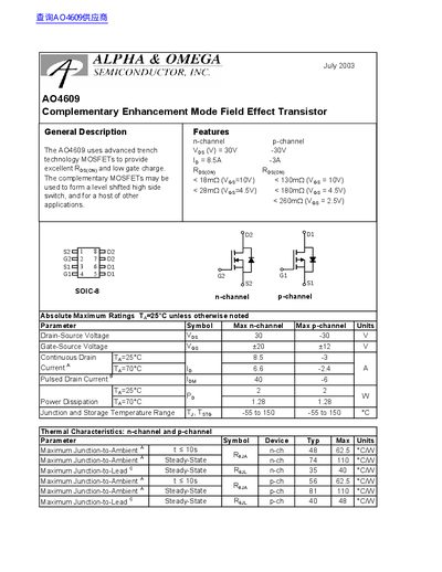
The AO4609 is a complementary enhancement‑mode MOSFET that uses advanced trench technology to achieve low on‑resistance and low gate charge. It is offered in both n‑channel and p‑channel versions and can be used for high‑side switching, level‑shifted circuits, and other applications.
The document lists absolute maximum ratings, detailed static and dynamic electrical characteristics, typical thermal performance curves, and mechanical data for the SO‑8 package, including tape‑and‑reel handling information. This manual is written in Chinese.
| Maximum Drain‑Source Voltage (VDS) | ±30 V |
|---|---|
| Continuous Drain Current (ID) | 8.5 A (n‑channel) / 3 A (p‑channel) |
| On‑Resistance (RDS(ON)) at VGS=10 V | < 18 mΩ (n‑channel) / < 130 mΩ (p‑channel) |
| Total Gate Charge (Qg) at VGS=10 V | 19.2 nC |
| Input Capacitance (Ciss) | 1040 pF (n‑channel) / 409 pF (p‑channel) |
| Package Type | SO‑8 |
The AO4609 is rated for a maximum drain‑source voltage of ±30 V.
The typical on‑resistance is less than 18 mΩ at VGS = 10 V.
The total gate charge is 19.2 nC when driven at 10 V.