
The document describes the features and characteristics of the AO4614 model p-channel and n-channel enhancement mode field effect transistors. It uses advanced trench technology MOSFETs to provide excellent RDS(ON) and low gate charge. The product can be used in H-bridge, inverters, and other applications.
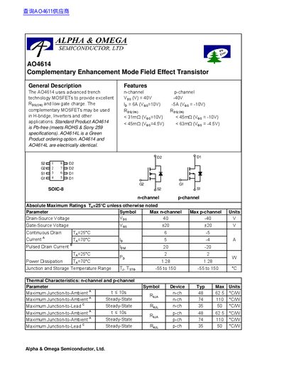
The AO4614 is a complementary enhancement mode field‑effect transistor that combines n‑channel and p‑channel trench MOSFET technology. It is offered as a RoHS‑compliant, Pb‑free device for use in H‑bridge, inverter and other power conversion applications.
The document provides absolute maximum ratings, detailed static and dynamic electrical characteristics for both n‑channel and p‑channel versions, and typical thermal performance curves. It also includes notes on measurement conditions, pulse rating limits, and a disclaimer regarding critical‑life‑support usage.
| Drain‑Source Voltage (VDS) Max | ±40 V |
|---|---|
| Gate‑Source Voltage (VGS) Max | ±20 V |
| Continuous Drain Current (Id) – N‑channel | 6 A (VGS=10 V) |
| Power Dissipation (PD) Max | 1.28 W |
| Input Capacitance (Ciss) – N‑channel | 404 pF |
| Input Capacitance (Ciss) – P‑channel | 657 pF |
The AO4614 can tolerate up to ±40 V drain‑source voltage.
The n‑channel version supports 6 A at VGS = 10 V, while the p‑channel version supports 5 A at the same gate voltage.
Yes, the standard product A04614 is Pb‑free and meets RoHS specifications.