
The AO4419 is a P-channel enhancement mode field effect transistor with low on-resistance and low gate charge, suitable for load switch or PWM applications.
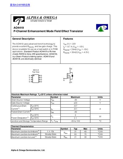
The AO4419 is a P‑Channel enhancement mode field‑effect transistor designed with advanced trench technology for low on‑resistance and low gate charge. It is suitable for load‑switch and PWM applications and is offered as a Pb‑free, RoHS‑compliant part, with a green‑product option AO4419L that is electrically identical.
The document provides absolute maximum ratings, electrical characteristics, thermal performance data, and switching parameters such as gate charge and turn‑on/off times. Typical graphs illustrate on‑region behavior, transfer characteristics, on‑resistance versus temperature and gate‑source voltage, and body‑diode performance.
| Drain‑Source Voltage (V_DSS) | -30 V |
|---|---|
| Gate‑Source Voltage (V_GS) | +20 V |
| Continuous Drain Current (I_D) at 25 °C | -9.7 A |
| Pulsed Drain Current | -40 A |
| Power Dissipation at 70 °C | 2.1 W |
| Junction‑to‑Ambient Thermal Resistance (RθJA) typical | 31 °C/W |
| Total Gate Charge at 10 V (Q_g) | 26.4 nC |
The AO4419 can withstand a drain‑source voltage of –30 V.
The device is rated for a continuous drain current of –9.7 A at 25 °C.
Yes, the standard AO4419 is Pb‑free and meets RoHS specifications.
The typical total gate charge at 10 V is 26.4 nC.