
AO4409 is a P-Channel Enhancement Mode Field Effect Transistor produced by Alpha & Omega Semiconductor, Ltd. It has a maximum power dissipation of 3W, a maximum working temperature of 150℃, a maximum working voltage of -30V, and a maximum working current of -15A. AO4409 uses advanced trench technology to provide excellent RDS(ON) and ultra-low low gate charge, making it suitable for use as a load switch or in PWM applications.
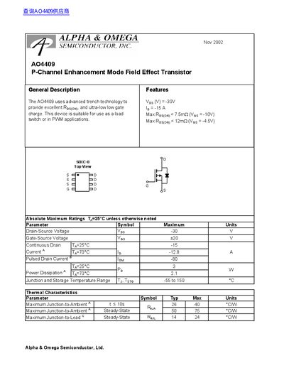
The AO4409 is a P‑Channel Enhancement Mode Field Effect Transistor designed for switching and PVVM applications. It uses trench technology to achieve low on‑resistance and low gate charge, making it suitable for high‑current load switching.
The document lists absolute maximum ratings, thermal characteristics, detailed electrical parameters such as drain‑source voltage, gate‑source voltage, continuous and pulsed drain currents, capacitances, and gate charge. Package information for the SOP‑8 and SO‑8 tape‑and‑reel formats is also provided.
| Drain‑Source Voltage (Vds) max | -30 V |
|---|---|
| Gate‑Source Voltage (Vgs) max | +20 V |
| Continuous Drain Current (Id) max | -15 A |
| Pulsed Drain Current (Id) max | -80 A |
| Input Capacitance (Ciss) | 5270 pF |
| Total Gate Charge (Qg) | 100 nC |
| Package Type | SOP‑8 |
The AO4409 can withstand a maximum drain‑source voltage of -30 V.
The typical input capacitance (Ciss) is 5270 pF.
The transistor is supplied in an SOP‑8 package.