
The AO4415 is a P-channel enhancement mode field effect transistor from Alpha & Omega Semiconductor, Ltd. Its features are RDS(ON) < 26mΩ (VGS = -20V), RDS(ON) < 35mΩ (VGS = -10V), and it is suitable for use as a load switch or in PWM applications.
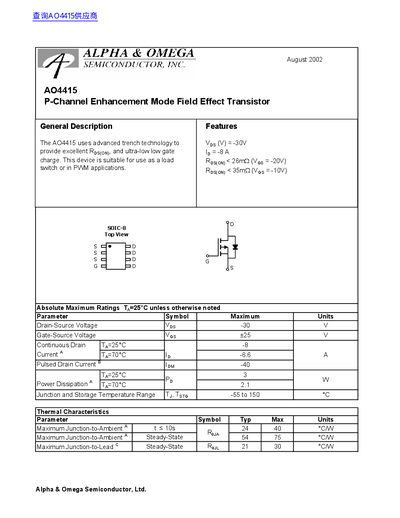
The AO4415 is a P‑Channel enhancement mode field‑effect transistor built with advanced trench technology. It is intended for use as a load switch or in PVVM applications, offering low on‑resistance and high current capability.
The document lists absolute maximum ratings, detailed electrical characteristics such as drain‑source voltage, gate‑source voltage, capacitances, and gate charge, as well as thermal performance data and mechanical dimensions for the SO‑8 package, including tape‑and‑reel handling information.
| Drain‑Source Voltage (VDS) max | -30 V |
|---|---|
| Gate‑Source Voltage (VGS) max | +25 V |
| Continuous Drain Current (ID) typ | 6.6 A |
| Pulsed Drain Current (ID) max | 40 A |
| Power Dissipation (PD) max | 2.1 W |
| Operating Temperature Range | -55 °C to 150 °C |
| Input Capacitance (Ciss) | 893 pF |
| Total Gate Charge (Qg) at 10 V | 16.6 nC |
| Package Part Number | AO4415 |
The AO4415 can tolerate a drain‑source voltage of up to –30 V.
The device is rated for a gate‑source voltage of up to +25 V.
The typical input capacitance is 893 pF.
The total gate charge is 16.6 nC when measured at 10 V.