
The MAX19538 is a 3.3V, 12-bit, 95Msps analog-to-digital converter (ADC) featuring a fully differential wideband track-and-hold (T/H) input amplifier, driving a low-noise internal quantizer. The analog input accepts single-ended or differential signals. The MAX19538 is optimized for low power, small size, and high dynamic performance. Excellent dynamic performance is maintained from baseband to input frequencies of 175MHz and beyond, making the MAX19538 ideal for intermediate frequency (IF) sampling applications. Powered from a single 3.3V supply, the MAX19538 consumes only 492mW while delivering a typical 68.4dB signal-to-noise ratio (SNR) performance at a 175MHz input frequency. In addition to low operating power, the MAX19538 features a 63µW power-down mode to conserve power during idle periods. A flexible reference structure allows the MAX19538 to use the internal 2.048V bandgap reference or accept an externally applied reference. The reference structure allows the full-scale analog input range to be adjusted from ±0.35V to ±1.10V. The MAX19538 provides a common-mode reference to simplify design and reduce external component count in differential analog input circuits. The MAX19538 supports either a single-ended or differential input clock drive. The internal clock duty-cycle equalizer accepts a wide range of clock duty cycles. Analog-to-digital conversion results are available through a 12-bit, parallel, CMOS-compatible output bus.
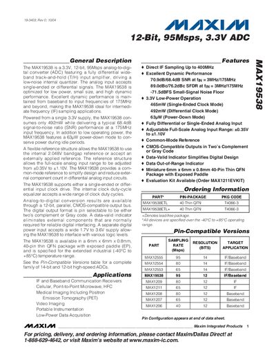
The MAX19538 is a 12‑bit, 95 Msps analog‑to‑digital converter optimized for low power, small size, and high dynamic performance. It operates from a single 3.3 V supply and offers both single‑ended and differential inputs with a flexible reference structure.
The device is supplied in a 40‑pin thin QFN package (6 mm × 6 mm × 0.8 mm) and is rated for an industrial temperature range of –40 °C to +85 °C. Detailed electrical characteristics, timing specifications, and package dimensions are provided in the datasheet.
| Resolution | 12 bits |
|---|---|
| Maximum Sampling Rate | 95 Msps |
| Supply Voltage | 3.3 V |
| Power Consumption (Differential Clock) | 492 mW |
| Power‑Down Current | 63 µW |
| Full‑Scale Input Range | +0.35 V to +1.10 V |
| Package | 40‑pin thin QFN 6 mm × 6 mm × 0.8 mm |
| Operating Temperature Range | –40 °C to +85 °C |
The MAX19538 can sample at up to 95 Msps.
It operates from a single 3.3 V supply.
In differential clock mode the device consumes about 492 mW.
It is available in a 40‑pin thin QFN package measuring 6 mm × 6 mm × 0.8 mm.