
The ADG3248 is a 2.5 V or 3.3 V, high performance 2:1 multiplexer/demultiplexer. It is designed on a low voltage CMOS process, which provides low power dissipation yet gives high switching speed and very low on resistance. The low on resistance allows level translation and bus switching at high data rates without introducing significant signal degradation. The device features low power consumption, high switching speed, and low on resistance.
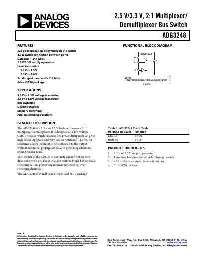
The ADG3248 is a high‑performance 2:1 multiplexer/demultiplexer designed on a low‑voltage CMOS process. It operates from a 2.3 V to 3.6 V supply, offers break‑before‑make switching, and is available in a tiny 6‑lead SC70 package.
Key specifications include a 0.225 ns propagation delay, 4.5 Ω on‑resistance, 1.244 Gbps maximum data rate, and operation over an industrial temperature range of –40 °C to +85 °C. The device supports mixed‑voltage level translation (3.3 V↔2.5 V and 2.5 V↔1.8 V) and is suited for bus switching, docking stations, memory banks, and analog switching applications.
| Supply Voltage Range | 2.3 V to 3.6 V |
|---|---|
| Propagation Delay | 0.225 ns |
| On‑Resistance | 4.5 Ω |
| Input Leakage Current | ±0.01 µA |
| Operating Temperature Range | –40 °C to +85 °C |
| Package | 6‑lead SC70 |
The device operates from 2.3 V up to 3.6 V.
The typical propagation delay is 0.225 ns.