
This document describes the features and characteristics of the ADN4691E/ADN4693E/ADN4696E/ADN4697E high-speed M-LVDS transceivers, including operating voltage, data transfer rate, half-duplex and full-duplex modes, etc.
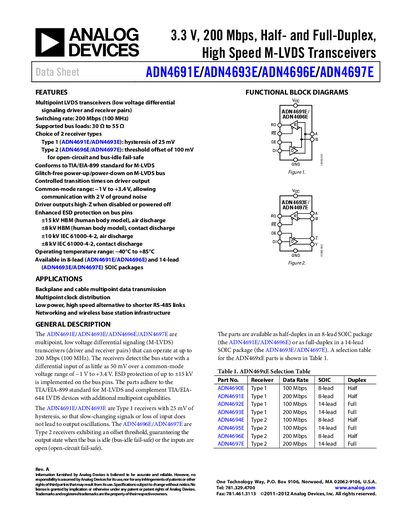
The ADN469xE family are multipoint low‑voltage differential signaling (M‑LVDS) transceivers that operate up to 200 Mbps and support both half‑ and full‑duplex modes. They offer robust ESD protection, fail‑safe bus‑idle behavior, and a common‑mode range that tolerates ground noise.
The handbook includes detailed specifications, timing diagrams, pin‑out tables, absolute maximum ratings, thermal resistance data, and typical performance curves to aid designers in integrating the devices into backplane, cable, and clock‑distribution applications.
| Maximum Data Rate | 200 Mbps |
|---|---|
| Differential Output Voltage Magnitude | 480‑650 mV |
| Operating Temperature Range | -40°C to +85°C |
| Supply Current (Only Driver Enabled) | 13‑22 mA |
| ESD Air Discharge Rating | +15 kV |
The device supports a maximum data rate of 200 Mbps.
The bus pins are protected up to +15 kV HBM (air discharge) and +8 kV HBM (contact discharge).