
The ADN4661 is a single-chip CMOS low-voltage differential signaling (LVDS) line driver that supports ±15 kV ESD protection, 600 Mbps (300 MHz) switching rates, 3.3 V power supply, ±355 mV differential signaling, low power consumption, and is suitable for backplane data transmission, cable data transmission, clock distribution and other applications
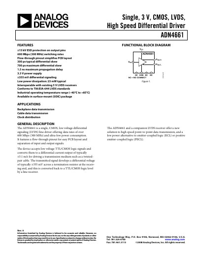
The ADN4661 is a single, CMOS, low‑voltage differential signaling (LVDS) line driver that converts a 3 V logic input into a differential current output. It features a flow‑through pinout for easy PCB layout, operates over a 3.0 V to 3.6 V supply range, and provides ±15 kV ESD protection on its output pins.
The datasheet includes detailed specifications such as a typical differential output voltage of 355 mV, propagation delay of 0.8 ns, and unloaded supply current of 4 mA. It also provides pin configurations, typical performance curves, and application examples for backplane and cable data transmission.
| Supply Voltage (VCC) | 3.0 V to 3.6 V |
|---|---|
| Typical Differential Output Voltage (VOD) | 355 mV |
| Unloaded Supply Current (ICC) | 4.0 mA typical |
| Typical Propagation Delay (tPHLD) | 0.8 ns |
| ESD Protection (output pins) | ±15 kV |
The typical differential output voltage is 355 mV.
It operates from 3.0 V to 3.6 V.
It supports data rates of over 600 Mbps (300 MHz).
The device offers ±15 kV ESD protection on the output pins.