
The ADN4665 is a 3V, LVDS, Quad, CMOS differential line driver. It has ±15kV ESD protection, 400 Mbps (200 MHz) switching rates, 100 ps typical differential skew, 400 ps maximum differential skew, 2 ns maximum propagation delay, 3.3 V power supply, ±350 mV differential signaling, low power dissipation (13 mW typical), interoperability with existing 5 V LVDS receivers, high impedance on LVDS outputs on power-down, compliance with TIA/EIA-644 LVDS standards, industrial operating temperature range of -40°C to +85°C, and is available in surface-mount SOIC package and low profile TSSOP package.
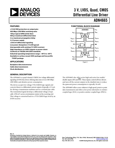
The ADN4665 is a quad‑channel, CMOS low‑voltage differential signaling (LVDS) line driver that converts single‑ended 3 V logic signals to differential current outputs. It supports data rates over 400 Mbps (200 MHz) and includes active high and low enable inputs for power‑down control. Key features include ±15 kV ESD protection, 400 Mbps switching, low propagation delay, and operation over an industrial temperature range of –40 °C to +85 °C. The device is offered in SOIC and TSSOP surface‑mount packages and complies with TIA/EIA‑644 LVDS standards.
| Supply Voltage (VCC) | 3.0 V to 3.6 V |
|---|---|
| Differential Output Voltage (VOD) – Typical | 350 mV |
| No‑Load Supply Current (ICC) – Drivers Enabled | 5.0 mA |
| ESD Protection on Output Pins | ±15 kV |
| Industrial Operating Temperature Range | −40 °C to +85 °C |
The typical no‑load supply current is about 5 mA, rising to around 23 mA under load.
It can operate at data rates of over 400 Mbps (200 MHz).
The device is a quad‑channel driver, providing four independent LVDS channels.