
ADN4666 is a 3.3V LVDS quad CMOS differential line receiver with ±8kV ESD IEC 61000-4-2 contact discharge, 400Mbps (200MHz) switching rates, 100ps channel-to-channel skew, 100ps differential skew, 3.3ns propagation delay, 3.3V power supply, high impedance outputs on power-down, low power design, 10 mW quiescent typical power consumption, interoperable with existing 5V LVDS drivers, supports small swing (350 mV typical) differential input signal levels, supports open, short, and terminated input fail-safe, conforms to TIA/EIA-644 LVDS standard, industrial operating temperature range of -40°C to +85°C, available in surface-mount SOIC package and low profile TSSOP package.
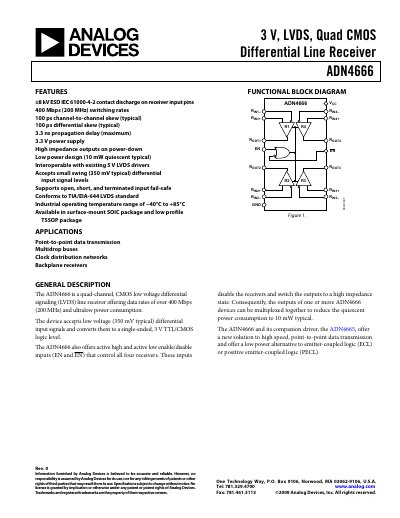
The ADN4666 is a quad‑channel, CMOS low‑voltage differential signaling (LVDS) line receiver that accepts 350 mV typical differential inputs and converts them to single‑ended 3 V TTL/CMOS logic levels. It features active high and low enable inputs, low‑power operation (≈10 mW typical), and compliance with the TIA/EIA‑644 LVDS standard.
The device operates from a 3.0 V‑3.6 V supply, supports data rates over 400 Mbps (200 MHz), and offers robust ESD protection (±8 kV IEC 61000‑4‑2). Typical specifications include output high voltage 2.7‑3.0 V, output low voltage 0.1‑0.25 V, and an industrial temperature range of –40 °C to +85 °C. Applications include point‑to‑point data transmission, mult‑drop buses, and clock distribution networks.
| Supply Voltage (VCC) | 3.0 V to 3.6 V |
|---|---|
| Maximum Data Rate | 400 Mbps (200 MHz) |
| Typical Quiescent Power | 10 mW |
| ESD Protection | ±8 kV IEC 61000‑4‑2 contact discharge |
| Operating Temperature Range | −40 °C to +85 °C |
| Output High Voltage (VOH) | 2.7 V to 3.0 V |
| Output Low Voltage (VOL) | 0.1 V to 0.25 V |
It supports data rates of over 400 Mbps (200 MHz) switching rates.
The device operates from a supply voltage of 3.0 V to 3.6 V.
Typical quiescent power consumption is about 10 mW.
It provides ±8 kV IEC 61000‑4‑2 contact discharge protection on the receiver input pins.