
The ADG3249 is a 2.5 V or 3.3 V, high performance 2:1 multi- plexer/demultiplexer bus switch. It is designed on a low voltage CMOS process, which provides low power dissipation yet gives high switching speed and very low on resistance. This allows the input to be connected to different voltage rails, thus achieving voltage translation.
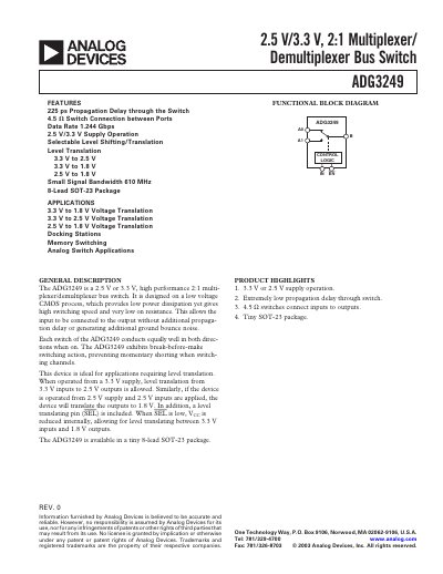
The ADG3249 is a high‑performance 2:1 multiplexer/demultiplexer bus switch built on a low‑voltage CMOS process. It operates from a 2.3 V to 3.6 V supply and offers selectable level‑shifting between 3.3 V, 2.5 V and 1.8 V domains. The device features break‑before‑make switching to prevent short‑circuit transients and is supplied in a compact 8‑lead SOT‑23 package.
Typical applications include voltage translation for docking stations, memory switching, and mixed‑voltage interfacing such as connecting a 3.3 V ADC to a 2.5 V microprocessor. The switch provides a propagation delay of about 0.225 ns, an on‑resistance of roughly 4.5 Ω, and supports data rates up to 1.244 Gbps, making it suitable for high‑speed analog and digital bus designs.
| Supply Voltage (VCC) | 2.3 V to 3.6 V |
|---|---|
| Propagation Delay | 0.225 ns |
| On‑Resistance (RON) | 4.5 Ω (typical) |
| Maximum Data Rate | 1.244 Gbps |
| Package | 8‑Lead SOT‑23 |
The device operates from a VCC of 2.3 V up to 3.6 V.
Typical propagation delay is about 0.225 ns.
The on‑resistance is roughly 4.5 Ω.
It can handle data rates up to 1.244 Gbps.