
This datasheet provides detailed information about 2.5 V/3.3 V, 2-Bit Common Control Level Translator Bus Switch ADG3242 Rev. A, including features, applications, pin diagram, etc.
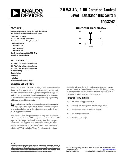
The ADG3242 is a low‑voltage CMOS digital switch that provides bidirectional level translation between 3.3 V, 2.5 V and 1.8 V domains. It features a common bus enable input, selectable level‑shifting, and a tiny 8‑lead SOT‑23 package.
Typical applications include voltage translation, bus isolation, hot‑plug and hot‑swap protection, and analog switching in video graphics or back‑plane bus architectures. Key performance figures are a 225 ps propagation delay, 4.5 Ω on‑resistance, and a maximum data rate of 1.5 Gbps.
| Propagation delay | 225 ps |
|---|---|
| On‑resistance (typical) | 4.5 Ω |
| Maximum data rate | 1.5 Gbps |
| Supply voltage (VCC) range | 2.3 V to 3.6 V |
The device has a propagation delay of 225 ps through the switch.
It operates from a VCC of 2.3 V to 3.6 V.
It is a 2‑bit, 2‑port common‑control digital switch.
The maximum data rate is 1.5 Gbps.