
ADN4662 is a single-channel, 3V, CMOS, LVDS differential line receiver from Analog Devices, which has ±15 kV ESD protection, 400 Mbps (200 MHz) switching rates, a simple PCB layout, 2.5 ns maximum propagation delay, 3.3 V power supply, high impedance outputs, and low power design.
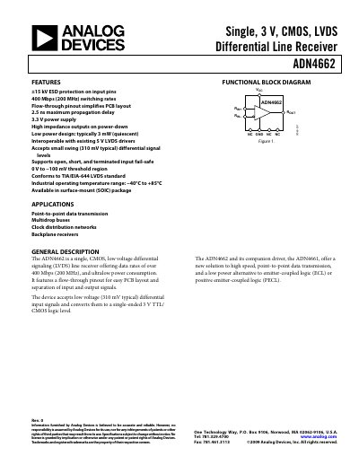
The ADN4662 is a single, CMOS, low‑voltage differential signaling (LVDS) line receiver offering data rates over 400 Mbps (200 MHz) and ultralow power consumption. It features a flow‑through pinout for easy PCB layout and accepts differential input signals as low as 310 mV typical, converting them to a 3 V TTL/CMOS logic level.
The device operates from a 3.0 V to 3.6 V supply, provides up to 2.5 ns propagation delay, and is protected by ±15 kV ESD on its input pins. It is rated for industrial temperature ranges from –40 °C to +85 °C and typically consumes only 3 mW of quiescent power.
| Maximum data rate | 400 Mbps (200 MHz) |
|---|---|
| Maximum propagation delay | 2.5 ns |
| Supply voltage (VDD) | 3.0 V to 3.6 V |
| Output high voltage (VOH) | 2.7 V to 3.1 V |
| ESD protection (input pins) | ±15 kV |
| Quiescent power consumption | typically 3 mW |
| Operating temperature range | –40 °C to +85 °C |
The device supports data rates of up to 400 Mbps (200 MHz).
It is rated for industrial temperatures from –40 °C to +85 °C.
Typical quiescent power consumption is about 3 mW.
All input pins are protected against ±15 kV human‑body model ESD.