
The ADN4664 is a dual-channel, 3V, CMOS, LVDS differential line receiver. It features 15kV ESD protection, 400Mbps (200MHz) switching rates, 100ps channel-to-channel skew (typical), 2.5ns maximum propagation delay, 3.3V power supply, high impedance outputs, low power design (typical 3mW), interoperability with existing 5V LVDS drivers, support for small swing (310mV typical) differential signal levels, support for open, short, and terminated input fail-safe, 0V to -100mV threshold region, compliance with TIA/EIA-644 LVDS standard, an industrial operating temperature range of -40°C to +85°C, and a surface-mount (SOIC) package.
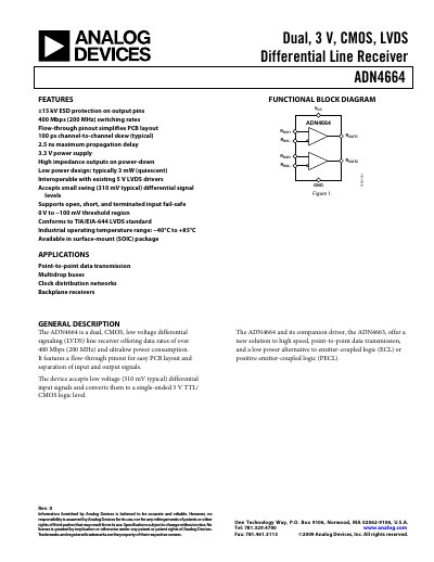
The ADN4664 is a dual, CMOS LVDS line receiver that converts a 310 mV differential input into a 3 V TTL/CMOS output. It features a flow‑through pinout, low‑power operation (typically 3 mW) and robust ESD protection.
Typical applications include point‑to‑point data transmission, multidrop buses, clock distribution and backplane receivers. The device operates from 3.0 V to 3.6 V, supports up to 400 Mbps (200 MHz) switching, and meets industrial temperature specifications of –40 °C to +85 °C.
| Supply voltage (VDD) | 3.0 V to 3.6 V |
|---|---|
| High input threshold (VTH) | +100 mV |
| Low input threshold (VTL) | −100 mV |
| Output high voltage (VOH) | 2.7 V–3.1 V |
| Output low voltage (VOL) | 0.3 V–0.5 V |
| No‑load supply current (ICC) | 5.4 mA–9 mA |
| Typical propagation delay (tPHLD) | 2.5 ns |
| Channel‑to‑channel skew | 100 ps (typical) |
| ESD protection | ±15 kV (output pins) |
| Industrial temperature range | −40 °C to +85 °C |
The device operates from 3.0 V to 3.6 V.
It supports data rates of over 400 Mbps (200 MHz).
The output pins are rated for ±15 kV human‑body model protection.
It is rated for industrial temperatures from –40 °C to +85 °C.