
The ADN4663 is a dual, CMOS, low voltage differential signaling (LVDS) line driver that offers 600 Mbps of high-speed transmission rates and a 3.3V power supply voltage. The driver features ±15 kV of ESD protection, 300 ps of typical differential skew and 1.5 ns of maximum propagation delay. It conforms to the TIA/EIA-644 LVDS standard and is interoperable with existing 5 V LVDS receivers. The driver is suitable for backplane data transmission, cable data transmission and clock distribution applications.
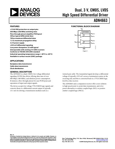
The ADN4663 is a dual, CMOS, low‑voltage differential‑signaling (LVDS) line driver that converts single‑ended TTL/CMOS inputs to a differential current output. It features a flow‑through pinout for easy PCB layout, ±15 kV ESD protection, and operates from a 3.0 V to 3.6 V supply.
Typical specifications include a differential output voltage of 250‑450 mV, propagation delays around 0.8 ns, and an unloaded supply current of about 14 mA. The device is intended for backplane, cable, and clock‑distribution applications where high‑speed, low‑power data transmission is required.
| Supply Voltage (VCC) | 3.0 V to 3.6 V |
|---|---|
| Differential Output Voltage (VOD) | 250 mV – 450 mV (typical 355 mV) |
| Supply Current (unloaded, ICC) | 8 mA – 14 mA |
| Differential Propagation Delay (typical) | 0.8 ns |
| Output Drive Current | ±2.5 mA to ±4.5 mA (typical ±3.55 mA) |
The device operates from 3.0 V to 3.6 V.
It supports data rates of over 600 Mbps (300 MHz).
Typical unloaded supply current is about 14 mA.