
The AD9523-1 is a low jitter clock generator with 14 LVPECL/LVDS/HSTL/29 LVCMOS outputs
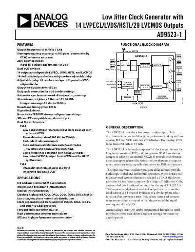
The AD9523-1 provides a low‑power, multi‑output clock distribution solution with configurable output standards and a zero‑delay operation. It integrates two PLLs, a VCO, and an on‑chip EEPROM for storing configuration settings. The device supports output frequencies from below 1 MHz up to 1 GHz and offers fine‑resolution adjustable delay for timing alignment.
Typical applications include LTE and multicarrier GSM base stations, wireless and broadband infrastructure, high‑speed ADC/DAC clocking, and 10 Gbps protocol timing. The datasheet details electrical specifications, pin configurations, serial control interfaces (SPI/I²C), and thermal considerations for board designers.
| Output frequency range | <1 MHz to 1 GHz |
|---|---|
| Start‑up frequency accuracy | <±100 ppm |
| Zero‑delay operation | Supported |
| Output‑to‑output skew | <50 ps |
| Absolute output jitter (122.88 MHz) | <150 fs |
| On‑chip VCO frequency range | 2940 MHz to 3100 MHz |
The device can generate outputs from less than 1 MHz up to 1 GHz.
The absolute output jitter is less than 150 fs at 122.88 MHz.