
AD9552 is a frequency upconverter produced by Analog Devices. It converts a low frequency input reference signal to a high frequency output signal. Input frequencies range from 6.6MHz to 112.5MHz, and output frequencies can reach 900MHz. It has preset pin programmable frequency translation ratios, arbitrary frequency translation ratios via SPI port, on-chip VCO, crystal resonator and/or external oscillator as a reference frequency source, secondary output (either integer-related to the primary output or a copy of the reference input), rms jitter: <0.5ps, SPI-compatible, 3-wire programming interface, single supply (3.3V), low power (under most conditions) <400 mW, and small package size (5mm x 5mm). It can effectively replace high frequency VCXO, OCXO and SAW resonators, and provide low jitter extremely flexible frequency translation for SONET/SDH.
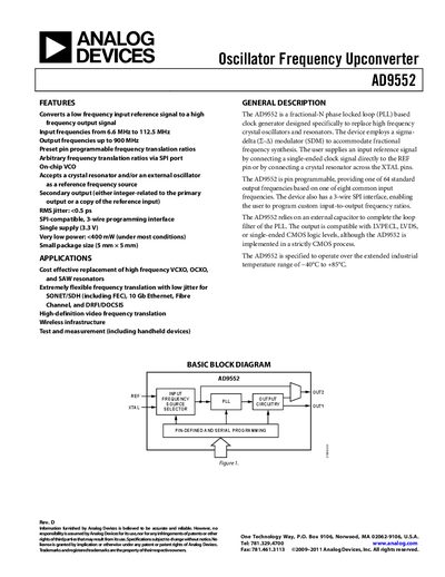
The AD9552 is a fractional‑N phase‑locked loop (PLL) based frequency upconverter that converts low‑frequency reference inputs (6.6 MHz‑112.5 MHz) to high‑frequency outputs up to 900 MHz. It offers pin‑programmable preset ratios and a 3‑wire SPI interface for custom frequency translation.
The document provides a complete set of specifications, pin descriptions, serial control timing, absolute maximum ratings, and application guidance for use in high‑speed communications, video, wireless infrastructure, and test equipment.
| Supply Voltage | 3.135 V – 3.465 V (typ 3.30 V) |
|---|---|
| Total Current Consumption | 149 mA – 169 mA (max output, both channels active) |
| Output Frequency Range | Up to 900 MHz |
| RMS Jitter | <0.5 ps |
| Operating Temperature Range | ‑40 °C to +85 °C |
The device operates from 3.135 V to 3.465 V, with a typical value of 3.30 V.
The AD9552 provides a 3‑wire SPI interface that allows programming of custom input‑to‑output frequency ratios, in addition to 64 preset ratios selectable via pins.
The AD9552 delivers RMS jitter of less than 0.5 ps.
The supply voltage must not exceed 3.6 V.