
ADCLK948 is a SiGe clock fanout buffer with 2 selectable differential inputs and 8 LVPECL outputs. It operates at a frequency of 4.8 GHz and has a broadband random jitter of 75 fs rms. The product also features on-chip input terminations and a 3.3V power supply.
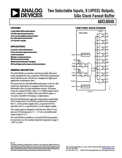
The ADCLK948 clock fanout buffer is fabricated on Analog Devices' proprietary XFCB3 SiGe bipolar process and is intended for high‑speed, low‑jitter applications such as clock distribution, signal restoration, level translation, and communications. It features two selectable differential inputs, on‑chip 100 Ω terminations, and eight full‑swing LVPECL output drivers.
The device operates from a 3.3 V supply, supports up to 4.8 GHz output frequency, and delivers 75 fs rms broadband random jitter. Detailed specifications, pin configurations, PCB layout guidelines, and thermal considerations are provided for designers.
| Maximum Output Frequency | 4.8 GHz |
|---|---|
| Broadband Random Jitter | 75 fs rms |
| Input Differential Range | 0.4 V to 3.4 V p‑p |
The ADCLK948 can operate up to 4.8 GHz.
The typical broadband random jitter is 75 fs rms.