
The document describes the features and characteristics of SiGe Clock Fanout Buffer ADCLK950 Rev. A, including 2 selectable inputs and 10 LVPECL outputs, operating frequency of 4.8 GHz, 75 fs rms broadband random jitter, on-chip input terminations. It is suitable for applications such as low jitter clock distribution, clock and data signal restoration, level translation, wireless communications, wired communications, medical and industrial imaging, ATE and high performance instrumentation.
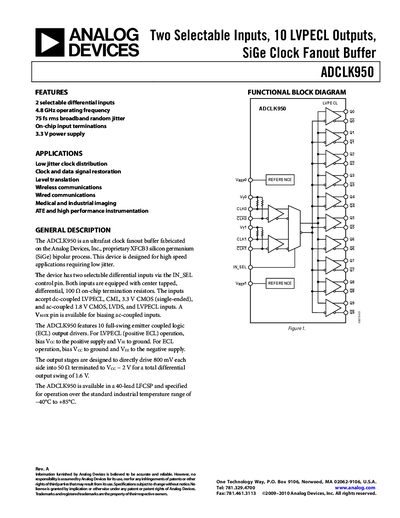
The ADCLK950 clock fanout buffer from Analog Devices provides two selectable differential inputs and ten full‑swing LVPECL outputs. It is fabricated on a SiGe bipolar process and is intended for high‑speed, low‑jitter applications such as clock distribution, data signal restoration, and level translation.
The device is supplied in a 40‑lead LFCSP package, operates over a –40 °C to +85 °C temperature range, and requires a 3.3 V supply. Detailed electrical characteristics, pin descriptions, and layout recommendations are included in this datasheet.
| Operating Frequency | 4.8 GHz |
|---|---|
| Broadband Random Jitter | 75 fs rms |
| Supply Voltage | 3.3 V ±10 % |
| Temperature Range | –40 °C to +85 °C |
| Output Differential Swing | 1.6 V (800 mV each side) |
| Package | 40‑lead LFCSP (CP‑40‑8) |
| Maximum Output Frequency | 45‑48 GHz |
The device operates at a frequency of 4.8 GHz.
It requires a 3.3 V supply with a ±10 % tolerance.
The ADCLK950 is rated for operation from –40 °C to +85 °C.
It provides ten full‑swing LVPECL output drivers.