
The AD9551 multiservice clock generator has the function of translating between any two standard network rates. It supports dual reference inputs and dual clock outputs, and can be programmed for standard network rate translation or arbitrary rational rate translation through pins or SPI. The output frequency range is from 10 MHz to 900 MHz, and the input frequency range is from 19.44 MHz to 806 MHz. It meets the OC-192 high band jitter requirement, supports standard forward error correction (FEC) rates, supports holdover operation, supports hitless switchover and phase build-out (even with unequal reference frequencies), has a SPI-compatible 3-wire programming interface, and operates on a single supply (3.3 V).
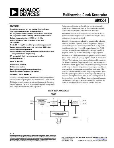
The AD9551 multiservice clock generator accepts one or two reference inputs and provides up to two clock outputs. It uses a fractional‑N PLL with an on‑chip VCO and supports both LVPECL, LVDS, and CMOS output levels. The device includes automatic reference switchover, holdover mode, and a 3‑wire SPI interface for arbitrary rational frequency ratios.
Key features include dual reference inputs, dual clock outputs, a single 3.3 V supply, an output frequency range up to 900 MHz, jitter as low as 0.5 ps rms, and operation over –40 °C to +85 °C. Detailed pin configurations, register maps, and electrical specifications are provided for system integration.
| Output frequency range | 0 – 900 MHz |
|---|---|
| Input frequency range | 19.44 MHz – 806 MHz |
| Supply voltage | 3.3 V (single supply) |
| Total current consumption (max output, both channels) | 195 mA |
| Operating temperature range | –40 °C to +85 °C |
| Reference inputs | Dual reference inputs |
| Programming interface | SPI‑compatible 3‑wire interface |
The AD9551 can generate clock outputs from 0 MHz up to 900 MHz.
It provides dual reference inputs that can be used simultaneously or as a backup.
The device is programmed via a 3‑wire SPI‑compatible serial control port.
The AD9551 operates from a single 3.3 V supply.