
AD9524 is a low-jitter clock generator with 6 LVPECL/LVDS/HSTL/13 LVCMOS outputs.
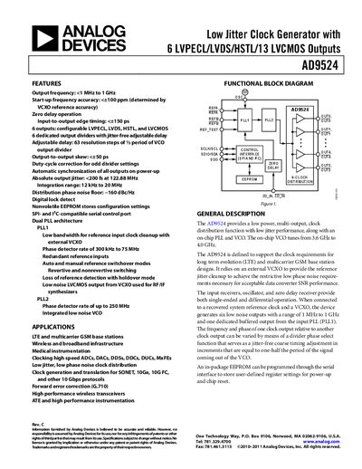
The AD9524 provides a low‑power, multi‑output clock distribution function with low jitter performance. It features a dual PLL architecture, an on‑chip VCO (3.6‑4.0 GHz), and six configurable outputs (LVPECL, LVDS, HSTL, LVCMOS) with adjustable delay and jitter‑free coarse timing.
Designed for LTE, GSM base stations, high‑speed data converters, and 10 Gbps protocols, the device includes a non‑volatile EEPROM for configuration storage and supports both SPI and I²C serial control interfaces.
| Output frequency range | <1 MHz to 1 GHz |
|---|---|
| Start‑up frequency accuracy | <+100 ppm |
| Input‑to‑output edge timing | <+150 ps |
| Absolute output jitter (122.88 MHz) | <200 fs |
| Integration range | 12 kHz to 20 MHz |
| Distribution phase‑noise floor | ‑160 dBc/Hz |
| Supply voltage (PLL1) | 3.3 V |
| Typical power dissipation (full load) | 571‑680 mW |
The AD9524 can generate output frequencies from less than 1 MHz up to 1 GHz.
It provides six outputs that can be configured as LVPECL, LVDS, HSTL, or LVCMOS.
The absolute output jitter is less than 200 fs at 122.88 MHz.
PLL1 operates from a 3.3 V supply.