
The ADCLK854 is a 1.2 GHz/250 MHz LVDS/CMOS fanout buffer optimized for low jitter and low power operation. Possible configurations range from 2 inputs/12 LVDS outputs to 2 inputs/24 CMOS outputs.
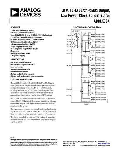
The ADCLK854 is a 1.2 GHz (LVDS) / 250 MHz (CMOS) fanout buffer optimized for low jitter and low power operation. It provides two selectable differential inputs and up to 12 LVDS or 24 CMOS outputs, with a sleep mode for power saving. Typical applications include clock distribution, data signal restoration, wireless and wired communications, and high‑performance instrumentation.
Key specifications include a supply voltage of 1.8 V, less than 12 mW per channel at 100 MHz, integrated jitter of 54 fs rms, and operation over an industrial temperature range of –40 °C to +85 °C. The device is offered in a 48‑lead LFCSP package with detailed pin‑out and control functions for LVDS/CMOS selection and sleep control.
| LVDS Output Frequency | 1200 MHz |
|---|---|
| CMOS Output Frequency | 250 MHz |
| Power Consumption per Channel | <12 mW (100 MHz operation) |
| Integrated Jitter | 54 fs rms |
| Propagation Delay (LVDS) | 2.0 ns |
| Output Rise/Fall Time (LVDS) | 135 ps (typical) |
| Operating Temperature Range | –40 °C to +85 °C |
It provides two selectable differential inputs.