
AD9523 Rev. B is a low jitter clock generator with 14 LVPECL/LVDS/HSTL and 29 LVCMOS outputs. It provides accurate output frequency and start-up frequency accuracy, zero delay operation, and precise input-to-output edge timing. It also features adjustable delay, output-to-output skew, automatic synchronization, and output dividers with jitter-free adjustable delay. The device has a low absolute output jitter and a wide integration range. It is controlled through a serial control port and has a dual PLL architecture.
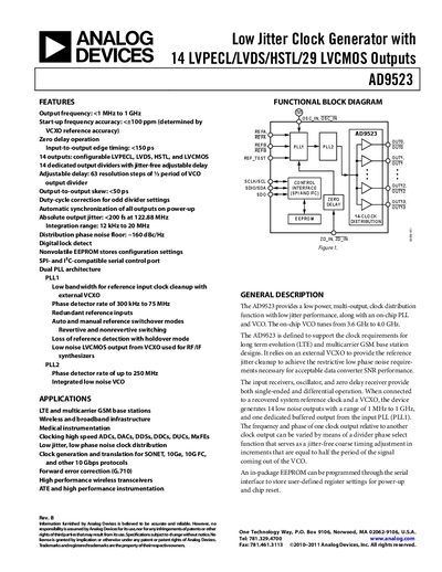
The AD9523 provides a low‑power, multi‑output clock distribution function with jitter‑free adjustable delay. It features a dual‑PLL architecture, an on‑chip VCO that tunes from 3.6 GHz to 4.0 GHz, and 14 configurable outputs supporting LVPECL, LVDS, HSTL, and LVCMOS standards.
Typical applications include LTE and multicarrier GSM base stations, high‑speed data converters, and 10 Gbps communication protocols. The device is supplied in a 72‑lead LFCSP package and includes an EEPROM for storing configuration settings.
| Output frequency range | <1 MHz to 1 GHz |
|---|---|
| Input‑to‑output edge timing | <150 ps |
| Output‑to‑output skew | <50 ps |
| Absolute output jitter (122.88 MHz) | <200 fs |
| Supply voltage VDD3_PLL1 (typical) | 3.3 V |
| Typical power dissipation (typical configuration) | 891 mW |
| Maximum output frequency (LVPECL mode) | 1 GHz |
The AD9523 supports output frequencies from less than 1 MHz up to 1 GHz.
It provides 14 outputs that can be configured as LVPECL, LVDS, HSTL, or LVCMOS.
Typical power dissipation is about 891 mW.