
This document is about the NC7SP08 technical data. NC7SP08 is a single 2-input AND gate from Fairchild's Ultra Low Power (ULP) Series of TinyLogic. Ideal for applications where battery life is critical, this prod- uct is designed for ultra low power consumption within the VCC operating range of 0.9V to 3.6V VCC. The internal circuit is composed of a minimum of inverter stages including the output buffer, to enable ultra low static and dynamic power.
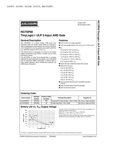
The NC7SP08 is a single 2‑Input AND gate from Fairchild's TinyLogic® Ultra Low Power (ULP) series, designed for battery‑critical applications with a supply range of 0.9 V to 3.6 V. It features a minimal inverter stage design for ultra‑low static and dynamic power consumption and operates with typical propagation delays as low as 2.5 ns at 3 V.
The document lists detailed electrical parameters, absolute maximum ratings, and mechanical dimensions for the 5‑lead SC70 (MAA05A) and 6‑lead MicroPak (MACO6A) packages, along with tape‑and‑reel handling specifications and ordering codes.
| Supply Voltage (VCC) | 0.9 V to 3.6 V |
|---|---|
| Typical Propagation Delay (3.0 V to 3.6 V) | 2.5 ns typ |
| Power‑Off Leakage Current | 0.05 µA |
| Input Capacitance | 0.2 pF |
| Output Capacitance | 0.4 pF |
| Operating Temperature Range | -65 °C to +150 °C |
The device operates with a supply voltage from 0.9 V to 3.6 V.
Typical propagation delay is 2.5 ns when VCC is between 3.0 V and 3.6 V.
Yes, the I/Os are tolerant up to 3.6 V when VCC is between 0.9 V and 3.6 V.