
This document describes the features and characteristics of the FDN361BN 30V N-Channel, Logic Level, PowerTrench® MOSFET. It is suitable for low voltage applications and provides fast switching and low power consumption.
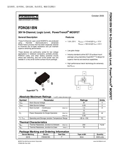
The FDN361BN is a 30 V N‑Channel Logic Level PowerTrench MOSFET designed for low‑voltage, battery‑powered applications such as notebooks and portable phones. It uses Fairchild's PowerTrench process and is offered in a SuperSOT‑3 surface‑mount package for superior thermal and electrical performance.
The datasheet provides absolute maximum ratings, electrical characteristics, typical on‑resistance curves, thermal resistance values, and recommended operating conditions. It also includes package marking information and links to Fairchild’s website for further reference.
| Drain‑Source Voltage (VDS) | 30 V |
|---|---|
| Gate‑Source Voltage (VGS) | +20 V |
| Continuous Drain Current (ID) | 1.4 A |
| Pulsed Drain Current (ID) | 10 A |
| Power Dissipation (PD) | 0.5 W |
| Junction‑to‑Ambient Thermal Resistance (RθJA) | 250 °C/W |
| Junction‑to‑Case Thermal Resistance (RθJC) | 75 °C/W |
| On‑Resistance (RDS(on)) @ VGS=10 V | 110 mΩ |
| On‑Resistance (RDS(on)) @ VGS=4.5 V | 160 mΩ |
The device is rated for a maximum drain‑source voltage of 30 V.
It can conduct up to 1.4 A continuously.
It is supplied in an industry‑standard SOT‑23 surface‑mount package using the proprietary SuperSOT‑3 design.
The datasheet is available on Fairchild Semiconductor’s website at www.fairchildsemi.com.