
This document describes the features and characteristics of the FDN358P P-Channel Logic Level Enhancement Mode Field Effect Transistor, released in March 1998. It includes information about its maximum voltage, maximum power dissipation, operating temperature range, etc.
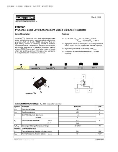
The Fairchild FDN358P is a P‑Channel logic‑level enhancement mode field‑effect transistor offered in a SuperSOT‑3 surface‑mount package. It is designed for low‑voltage, battery‑powered applications such as notebook computers and portable devices, providing fast switching and low on‑state resistance.
The document provides absolute maximum ratings, detailed electrical parameters, switching and thermal characteristics, as well as typical performance curves for drain‑source voltage, on‑resistance, gate charge and capacitance.
| Drain‑Source Voltage (VDS) | -30 V |
|---|---|
| Gate‑Source Voltage (VGS) | +20 V |
| Continuous Drain Current (ID) | 15 A |
| Pulsed Drain Current (ID,pulse) | 5 A |
| Maximum Power Dissipation | 0.5 W |
| Operating Temperature Range | -55 °C to 150 °C |
The device is rated for a maximum drain‑source voltage of -30 V.
It can conduct a continuous drain current of 15 A.
The transistor operates from -55 °C up to 150 °C.