
This document describes the features and characteristics of a P-Channel Logic Level MOSFET. The MOSFET is produced using advanced Power Trench process, which minimizes the on-state resistance and maintains low gate charge for superior switching performance. It is well suited for portable electronics applications such as load switching and power management, battery charging circuits, and DC/DC conversion.
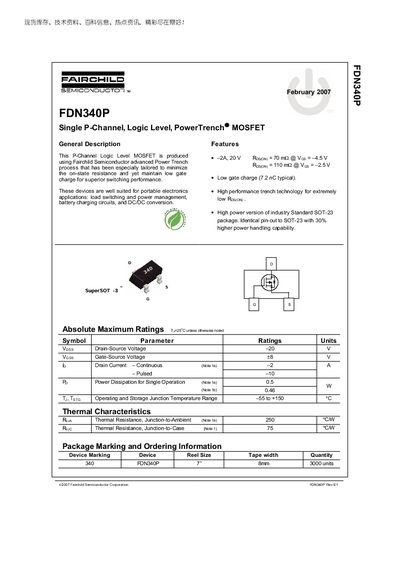
The FDN340P is a single P‑channel logic‑level PowerTrench MOSFET designed for portable electronics such as load switching, power management, battery charging, and DC/DC conversion. It is manufactured using Fairchild Semiconductor's advanced Power Trench process to achieve low on‑state resistance and low gate charge.
Key specifications include a -20 V drain‑source breakdown voltage, +8 V gate‑source rating, -2 A continuous drain current, 0.5 W power dissipation, and thermal resistances of 250 °C/W (junction‑to‑ambient) and 75 °C/W (junction‑to‑case). Typical gate charge is 7.2 nC, with input and output capacitances of 779 pF and 121 pF respectively.
| Drain-Source Voltage (V_DSS) | -20 V |
|---|---|
| Gate-Source Voltage (V_GS) | +8 V |
| Typical Gate Charge (Q_g) | 7.2 nC |
| Gate‑Drain Charge (Q_gd) | 1.5 nC |
The FDN340P is rated for a maximum drain‑source voltage of -20 V.
The typical gate charge is 7.2 nC.