
This document is about FDN352AP's technical information. The product is a P-channel MOSFET with extremely low R DS(ON) and SOT-23 package. It is suitable for low voltage and battery powered applications
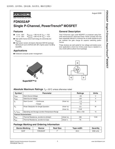
The FDN352AP is a single P‑Channel PowerTrench MOSFET designed for low‑voltage, battery‑powered applications where minimal in‑line power loss is required. It features a high‑performance trench structure that provides very low on‑state resistance while keeping gate charge low for fast switching. The device is offered in a high‑power SOT‑23 (SuperSOT‑3) package with a 30 % higher power handling capability than standard SOT‑23 parts.
The datasheet lists absolute maximum ratings, electrical characteristics, thermal data, and typical performance curves. Key parameters include a -30 V drain‑source breakdown voltage, -1.3 A continuous drain current, 0.5 W power dissipation, and junction‑to‑ambient thermal resistance of 250 °C/W. Detailed capacitance, gate‑charge, and switching timing specifications are provided for circuit designers.
| Drain‑Source Voltage (VDS) | -30 V |
|---|---|
| Gate‑Source Voltage (VGS) | 425 V |
| Continuous Drain Current (ID) | -1.3 A |
| Pulsed Drain Current (ID, pulsed) | -10 A |
| Power Dissipation (PD) | 0.5 W |
| Junction‑to‑Ambient Thermal Resistance (RθJA) | 250 °C/W |
| Junction‑to‑Case Thermal Resistance (RθJC) | 75 °C/W |
| Output Capacitance (Coss) | 40 pF |
| Total Gate Charge (Qg) | 1.4–1.9 nC |
The device is rated for a maximum drain‑source voltage of -30 V.
The continuous drain current rating is -1.3 A.