
This document describes the features and characteristics of the FQP13N50/FQPF13N50 500V N-Channel MOSFET products, including minimal on-state resistance, superior switching performance, and high energy pulse withstand capability. Suitable for high efficiency switch mode power supply, power factor correction, and half bridge electronic lamp ballast applications.
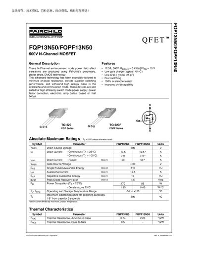
The FQP13N50 and FQPF13N50 are N‑Channel enhancement‑mode power MOSFETs fabricated with Fairchild’s planar‑stripe DMOS technology. They are optimized for low on‑state resistance, fast switching, and high‑energy avalanche capability, making them suitable for switch‑mode power supplies, power‑factor correction, and electronic lamp ballast applications.
Key electrical characteristics include a 500 V drain‑source rating, 12.5 A continuous drain current, typical on‑resistance of 0.48 Ω, low gate charge (≈45 nC), and modest input/output capacitances. The devices are offered in TO‑220 and TO‑220F packages with detailed thermal resistance and package dimensions provided.
| Drain‑Source Voltage (V_DSS) | 500 V |
|---|---|
| Continuous Drain Current (I_D) at 25 °C | 12.5 A |
| Gate Charge (Q_g) | 45 nC (typical) |
| Reverse Transfer Capacitance (C_rss) | 25 pF (typical) |
| Power Dissipation (P_D) at 25 °C | 170 W (FQP13N50), 56 W (FQPF13N50) |
| Thermal Resistance Junction‑to‑Case | 0.74 °C/W (FQP13N50), 2.23 °C/W (FQPF13N50) |
The FQP13N50 is rated for a maximum drain‑source voltage of 500 V.
Both devices have a typical gate charge of about 45 nC.
Fairchild states that its products are not authorized for use as critical components in life‑support devices without written approval.