
BSS139 is a N-channel MOSFET device produced by STMicroelectronics. Its maximum rated voltage is 250V, maximum continuous current is 0.1A, maximum pulsed current is 0.4A, minimum gate threshold voltage is -1.4V, and maximum drain-source on-resistance is 30Ω.
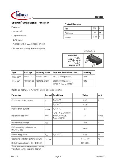
The BSS139 is an N‑channel small‑signal MOSFET with depletion‑mode operation, offering low on‑state resistance and fast switching characteristics. Key features include a continuous drain current of 0.10 A at 25 °C, a drain‑source breakdown voltage of 250 V, and a typical gate threshold voltage around –1.4 V.
The device is supplied in a PG‑SOT‑23 package, with detailed ratings for power dissipation (0.36 W at 25 °C), thermal resistance, and safe operating area. The datasheet also includes dynamic parameters such as input, output, and reverse transfer capacitances, as well as gate charge characteristics for design reference.
| Continuous drain current (Id) at 25 °C | 0.10 A |
|---|---|
| Power dissipation (Pd) at 25 °C | 0.36 W |
| Package type | PG‑SOT‑23 |
The BSS139 can handle a continuous drain current of 0.10 A at 25 °C.
The device is supplied in a PG‑SOT‑23 surface‑mount package.
The maximum power dissipation is 0.36 W at 25 °C.