
This document describes the features and characteristics of the SPP20N65C3, SPA20N65C3, and SPI20N65C3 Cool MOS™ power transistors, including worldwide best RDS(on), ultra-low gate charge, periodic avalanche rating, extreme dv/dt rating, high peak current capability, and improved transconductance.
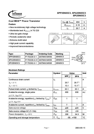
This datasheet provides the electrical, thermal and mechanical specifications for Infineon's high‑voltage power MOSFETs SPP20N65C3, SPA20N65C3 and SPI2Z0N65C3. It includes maximum ratings, characteristic curves, and typical performance graphs for designers.
Key sections cover features, maximum ratings, thermal characteristics, electrical characteristics, transient thermal impedance, and safety/legal notices. The document is intended for engineers selecting the device for high‑voltage, high‑current applications.
| Drain‑Source breakdown voltage (VDS) | 650 V |
|---|---|
| Continuous drain current (Id) at 25 °C | 20.7 A |
| Power dissipation at 25 °C (Pd) | 34.5 W |
The device can conduct a continuous drain current of 20.7 A at 25 °C.
The MOSFET is rated for a drain‑source breakdown voltage of 650 V.