
This document describes the features and characteristics of the 2SK2625LS model, including low ON-resistance and low Qg.
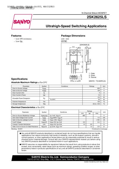
The 2SK2625LS is an N‑channel silicon MOSFET designed for ultrahigh‑speed switching applications. It offers low on‑resistance and low gate charge, making it suitable for high‑frequency power conversion and switching circuits.
The document lists absolute maximum ratings, electrical characteristics, and typical performance parameters such as a 600 V drain‑to‑source voltage, 4 A continuous drain current, and a typical on‑state resistance of about 2 mΩ. Safety notices, export‑control information, and usage guidelines are also included.
| Drain-to-Source Voltage (VDS) | 600 V |
|---|---|
| Gate-to-Source Voltage (VGS) | +30 V |
| Continuous Drain Current (ID, DC) | 4 A |
| Pulse Drain Current (ID, Pulse) | 16 A |
| Input Capacitance (Ciss) | 700 pF |
| Output Capacitance (Coss) | 220 pF |
| Reverse Transfer Capacitance (Crss) | 110 pF |
| Total Gate Charge (Qg) | 20 nC |
The device is rated for a maximum drain‑to‑source voltage of 600 V.
It can conduct up to 4 A of continuous drain current (DC).