
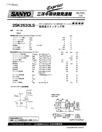
The 2SK2633LS is an N‑channel MOSFET designed for high‑speed switching applications. It features low on‑resistance and low gate charge, making it suitable for efficient power conversion.
The datasheet provides absolute maximum ratings, detailed electrical characteristics, switching time measurements, and package dimensions for the TO‑220F housing. This manual is written in Japanese.
| Drain‑Source Voltage (V_DSS) | 800 V |
|---|---|
| Gate‑Source Voltage (V_GSS) | ±80 V |
| Continuous Drain Current (I_D,DC) | 8 A |
| Pulsed Drain Current (I_D,pp) | 9 A |
| Power Dissipation (P_D) | 30 W |
| Maximum Channel Temperature (T_CH) | 150 °C |
| Storage Temperature Range (T_STG) | -55 °C to 150 °C |
| Gate‑Source Leakage Current (I_GSS) | 100 nA |
| Input Capacitance (C_iss) | 700 pF |
| Output Capacitance (C_oss) | 180 pF |
| Reverse Transfer Capacitance (C_rss) | 100 pF |
The device can withstand a drain‑source voltage of up to 800 V.
It is supplied in a TO‑220F (TO‑220) package.
The continuous drain current is 8 A and the pulsed drain current rating is 9 A.