
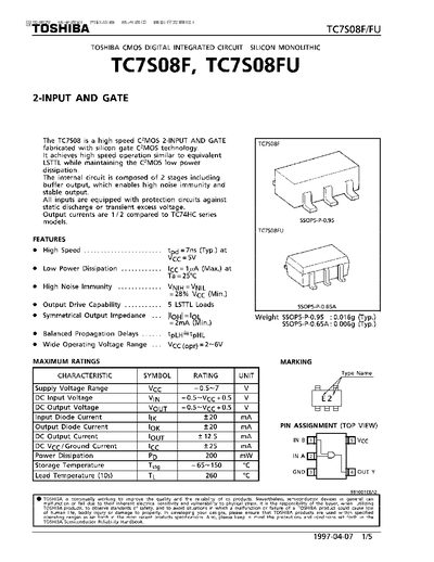
The TC7S08F/FU is a high‑speed CMOS 2‑input AND gate with low power dissipation, designed for LSTTL‑compatible operation. It features a buffered output stage for high noise immunity and includes protection against static discharge on all inputs.
The datasheet provides detailed maximum ratings, recommended operating conditions, DC and AC electrical characteristics, as well as package dimensions and outline drawings for the SSOP5‑P‑0.95 and SSOP5‑P‑0.65A packages.
| Low power dissipation (Icc max) | 14 µA (Max.) at Ta=25°C |
|---|---|
| Operating voltage range (Vcc) | 2 V to 6 V |
| Supply voltage range (VEE) | -0.5 V to 7 V |
| Input diode current (Iik) | +20 mA |
| Lead temperature (10 s) | 260 °C |
| Package weight (SSOP5‑P‑0.95) | 0.016 g (Typ.) |
| Package weight (SSOP5‑P‑0.65A) | 0.006 g (Typ.) |
It operates with a supply voltage (Vcc) from 2 V to 6 V.
The device is rated for a supply voltage (VEE) from –0.5 V to 7 V.
The maximum supply current is 14 µA at 25 °C.