
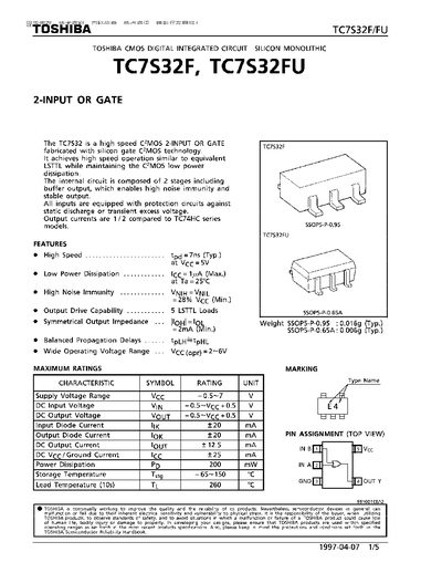
The TC7S32F/FU is a high‑speed C2MOS 2‑input OR gate with low power dissipation and high noise immunity. It features a buffered output stage, static‑discharge protection on inputs, and can drive up to five LSTTL loads.
The datasheet lists electrical characteristics such as a typical propagation delay of 7 ns, a supply voltage range of 2 V to 6 V, and a maximum power dissipation of 200 mW. Mechanical details include SSOP5‑P package dimensions and typical weight.
| Supply voltage range | 2 V to 6 V |
|---|---|
| Operating temperature range | -40 °C to 85 °C |
| Output drive capability | 5 LSTTL loads |
| Power dissipation | 200 mW |
| Maximum DC output current | 125 mA |
It operates from 2 V to 6 V.
The output can drive up to five LSTTL loads.
The device can source up to 125 mA of DC output current.