
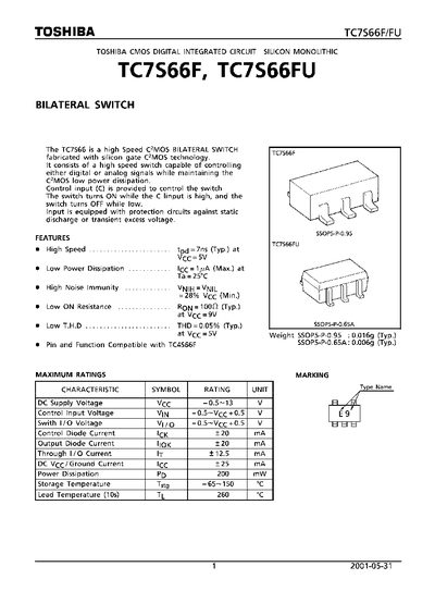
The TC7S66F/FU is a CMOS digital integrated circuit bilateral switch designed for high‑speed switching of digital or analog signals while maintaining low power dissipation. It features a typical propagation delay of 7 ns at a 5 V supply and a low on‑resistance of 1 kΩ at 9 V.
The datasheet provides maximum ratings, recommended operating conditions, DC and AC electrical characteristics, analog switch performance, package dimensions for SSOP5‑P‑0.95 and SSOP5‑P‑0.65, and usage restrictions for safety‑critical applications.
| Typical Propagation Delay | 7 ns (Typ.) at Vcc = 5 V |
|---|---|
| Typical On‑Resistance (Ron) | 1000 Ω (Typ.) at Vcc = 9 V |
| Maximum Power Dissipation | 200 mW |
| Supply Voltage Range | -0.5 V to 13 V |
| Control Input Voltage Range | -0.5 V to Vcc + 0.5 V |
| Operating Temperature | -40 °C to 85 °C |
The typical propagation delay is 7 ns at a supply voltage of 5 V.
The device can dissipate up to 200 mW.
The supply voltage may range from –0.5 V to 13 V.
The SSOP5‑P‑0.95 package measures 2.1 mm × 0.95 mm.