
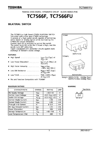
The TC7S66F/FU is a CMOS bilateral switch designed for high‑speed digital or analog signal control while maintaining low power consumption. It features a control input that turns the switch on when high and off when low, with built‑in protection against static discharge and transient voltages.
Key specifications include a typical propagation delay of 7 ns, ON resistance of 1 kΩ at 9 V, total harmonic distortion of 0.05 % at 5 V, and a supply voltage range of –0.5 V to 13 V. The device is supplied in SSOP5‑P packages (0.95 mm and 0.65 mm) with typical weights of 0.016 g and 0.006 g respectively. Toshiba advises that the part is intended for general electronics applications and should not be used in safety‑critical or high‑reliability systems such as medical or aerospace equipment.
| Typical propagation delay | 7 ns |
|---|---|
| Maximum supply current (Icc) | 1 A |
| ON resistance (typical) | 1 kΩ at Vcc=9 V |
| Total Harmonic Distortion (typical) | 0.05 % at Vcc=5 V |
| Supply voltage range | -0.5 V to 13 V |
| Power dissipation | 200 mW |
| Package weight (typical) | 0.016 g (SSOP5‑P‑0.95) |
The typical propagation delay is 7 ns.
The ON resistance is 1 kΩ typical at a supply voltage of 9 V.
The device is rated for a supply voltage from –0.5 V up to 13 V.