
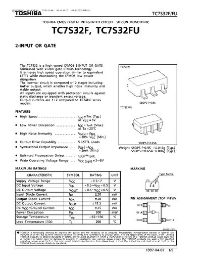
The TC7S32F/FU is a high‑speed C2MOS 2‑input OR gate that combines LSTTL‑level speed with low power consumption. It features a buffered output stage for high noise immunity and stable output, and includes input protection against static discharge and transient voltage.
The device is supplied in SSOP5‑P packages (0.95 mm and 0.65 mm pitch) with a typical weight of 0.016 g. Electrical specifications include a typical propagation delay of 7 ns, a supply voltage range of 2 V to 6 V, and the ability to drive up to five LSTTL loads. Power dissipation is limited to 200 mW.
| Typical propagation delay | 7 ns |
|---|---|
| Supply voltage range | 2 V – 6 V |
| Output drive capability | 5 LSTTL loads |
| Power dissipation | 200 mW |
| Typical weight (SSOP5‑P‑0.95) | 0.016 g |
The typical propagation delay is 7 ns.
It operates from 2 V to 6 V.
It can drive up to five LSTTL loads.
The device can dissipate up to 200 mW.