
This document describes the features and performance of the power MOSFET products, STP6NB25 and STP6NB25FP, produced by STMicroelectronics. These products utilize the latest high voltage MESH OVERLAY process and offer extremely high dv/dt capability, 100% avalanche tested, very low intrinsic capacitances, and minimized gate charge. They are suitable for high current, high speed switching, UPS, DC-DC & DC-AC converters for telecom, industrial, and consumer environments.
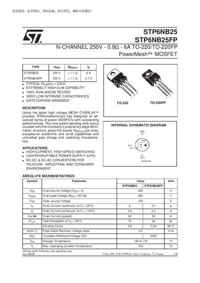
The STP6NB25 and STP6NB25FP are N‑channel 250 V power MOSFETs built with STMicroelectronics' PowerMesh™ MESH OVERLAY™ process. They offer extremely low on‑resistance, high avalanche capability and fast switching, making them suitable for high‑current, high‑speed applications such as UPS, DC‑DC and DC‑AC converters for telecom, industrial and consumer markets.
Key specifications include a typical Rds(on) of 0.9 mΩ, continuous drain current up to 6 A (3.7 A for the FP version) at 25 °C, total dissipation of 75 W (30 W for FP), and robust thermal performance with a junction‑to‑case resistance of 1.66 °C/W. The devices also feature low gate charge, high dv/dt capability and are fully avalanche‑tested.
| Drain‑source Voltage (Vds) | 250 V |
|---|---|
| Continuous Drain Current (Id) @ 25 °C | 6 A (STP6NB25) / 3.7 A (STP6NB25FP) |
| Total Dissipation (Pd) @ 25 °C | 75 W (STP6NB25) / 30 W (STP6NB25FP) |
| Typical On‑Resistance (Rds(on)) | 0.9 mΩ |
| Avalanche Current | 6 A |
| Thermal Resistance Junction‑case (RθJC) | 1.66 °C/W (TO‑220) / 4.17 °C/W (TO‑220FP) |
| Input Capacitance (Ciss) | 260 pF |
| Output Capacitance (Coss) | 68 pF |
| Reverse Recovery Time (trr) | 160 ns |
| Storage Temperature Range | -60 °C to 150 °C |
The maximum drain‑source voltage is 250 V.
The typical on‑resistance is 0.9 mΩ.
It can handle up to 6 A (3.7 A for the FP version) continuously at 25 °C.
They are suited for high‑current, high‑speed switching, UPS systems, and DC‑DC & DC‑AC converters in telecom, industrial and consumer environments.