
This document describes the features and characteristics of the N-channel enhancement mode fast power MOS transistors of STP6NA80 and STP6NA80FI models, including low RDS(on) and gate charge, unmatched ruggedness, and superior switching performance.
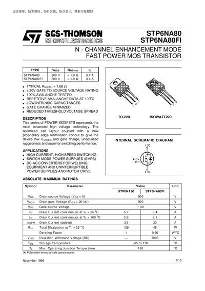
The STP6NA80 and STP6NA80FI are high‑voltage, fast‑switching power MOSFETs offered in TO‑220 ISOWATT220 and TO‑220 packages. They feature low on‑resistance, minimized gate charge, and robust avalanche capability for demanding applications such as SMPS, motor drives, and welding equipment.
The document provides absolute maximum ratings, thermal characteristics, detailed electrical parameters, switching performance data, mechanical dimensions, and test circuit diagrams to aid designers in integrating these devices into high‑power systems.
| Drain‑source voltage (VDS) max | 800 V |
|---|---|
| Gate‑source voltage rating | +30 V |
| Continuous drain current (ID) at 25 °C | 5.7 A (STP6NA80) / 3.4 A (STP6NA80FI) |
| Total power dissipation at 25 °C | 125 W (STP6NA80) / 45 W (STP6NA80FI) |
| Typical on‑resistance (RDS(on)) | 1.68 mΩ |
| Total gate charge (Qg) | 58 nC (typical) |
| Thermal resistance junction‑to‑case | 2.78 °C/W (max) |
Both devices are supplied in TO‑220 ISOWATT220 and standard TO‑220 packages.
The MOSFETs are rated for a maximum drain‑source voltage of 800 V.
At 25 °C the STP6NA80 can conduct up to 5.7 A continuously.