
STP6NB50/STP6NB50FP are N-channel enhancement mode MOSFETs from SGS-Thomson, which uses Mesh Overlay process and has extremely low on-resistance, high dv/dt capability, very low intrinsic capacitances and minimized gate charge, suitable for high current, high speed switching applications such as switch mode power supplies, welding equipment and motor drive
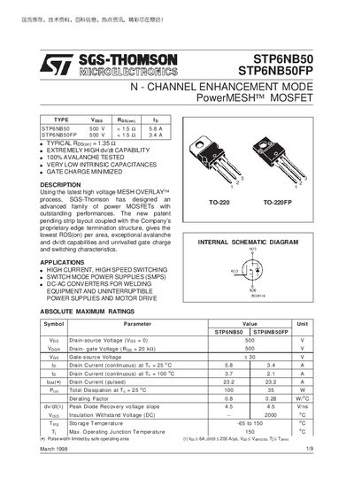
This datasheet describes the STP6NB50 and STP6NB50FP power MOSFETs, highlighting their high‑voltage capability, low on‑resistance and fast switching performance. It includes absolute maximum ratings, typical electrical characteristics, and thermal data for both the TO‑220 and TO‑220FP packages.
Mechanical dimensions, thermal impedance curves, and gate‑charge characteristics are also presented, together with safety notices and corporate information. The document is intended for designers and engineers selecting MOSFETs for SMPS, welding converters, UPS and motor‑drive applications.
| Drain‑source voltage (VDS) | 500 V |
|---|---|
| Gate‑source voltage (VGS) | 30 V |
| Continuous drain current (ID) @ 25 °C | 5.8 A (STP6NB50) / 3.4 A (STP6NB50FP) |
| Total power dissipation @ 25 °C | 100 W (STP6NB50) / 35 W (STP6NB50FP) |
| Output capacitance (Coss) | 110 pF (typ) / 149 pF (max) |
| Junction‑case thermal resistance | 1.25 °C/W (STP6NB50) / 3.57 °C/W (STP6NB50FP) |
| Maximum lead temperature for soldering | 300 °C |
The MOSFETs are rated for a maximum drain‑source voltage of 500 V.
At 25 °C the STP6NB50 can conduct 5.8 A continuously (STP6NB50FP 3.4 A).
The total dissipation is up to 100 W for the STP6NB50 and 35 W for the STP6NB50FP.