
This document describes the features and characteristics of the STP6NB50 and STP6NB50FP N - CHANNEL ENHANCEMENT MODE PowerMESH MOSFETs, including low RDS(on), extremely high dv/dt capability, 100% avalanche tested, very low intrinsic capacitances, and minimized gate charge.
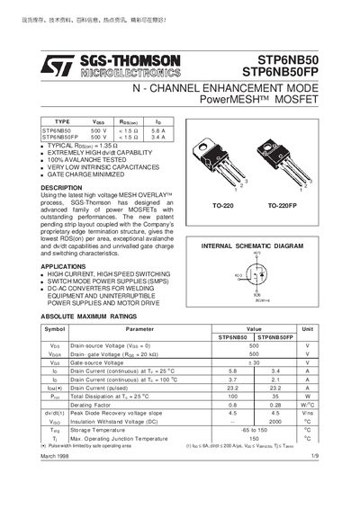
The STP6NB50 and STP6NB50FP are high‑voltage, low‑on‑resistance MOSFETs in TO‑220 and TO‑220FP packages. They are designed for high‑current, high‑speed switching applications such as SMPS, DC‑AC converters, welding equipment, UPS and motor drives.
Key specifications include a 500 V drain‑source rating, up to 5.8 A continuous drain current, typical RDS(on) of 1.35 mΩ, avalanche capability of 5.8 A, and a maximum junction temperature of 150 °C. Detailed thermal resistance, gate charge, and capacitance data are provided for design optimization.
| Drain‑source Voltage (VDS) | 500 V |
|---|---|
| Continuous Drain Current (ID) at 25 °C | 5.8 A (STP6NB50) / 3.4 A (STP6NB50FP) |
| Typical On‑Resistance (RDS(on)) | 1.35 mΩ |
| Avalanche Current | 5.8 A |
| Total Power Dissipation (PD) | 100 W (STP6NB50) / 35 W (STP6NB50FP) |
| Maximum Junction Temperature (Tj) | 150 °C |
| Gate Charge (Qg) | 21 nC (typical) |
| Input Capacitance (Ciss) | 680 pF |
| Output Capacitance (Coss) | 110 pF |
| Junction‑to‑Case Thermal Resistance (RθJC) | 1.25 °C/W (TO‑220) |
Both devices are rated for a maximum drain‑source voltage of 500 V.
The typical RDS(on) for the STP6NB50 is 1.35 mΩ at VGS = 10 V.
The STP6NB50 can dissipate up to 100 W at 25 °C.
The junction‑to‑case thermal resistance is 1.25 °C/W and the junction‑to‑ambient resistance is 62.5 °C/W.